 Home Home |
| For authors |
| Submission status |
| Current
|
| Archive
|
| Archive
(English)
|
| Search |
Self-assembled Ge quantum dots epitaxially grown on Si are of particular interest as they are fully compatible with Si-CMOS and can be applied for 1.3– 1.55 µm optical communication applications. Despite the recent progress in fabrication of near-infrared Ge/Si quantum dot photodetectors, their quantum efficiency still remains a major challenge and different approaches to improve the quantum dot photoresponse are under investigation. It was recently demonstrated that the integration of Ge/Si heterostructures with arrays of metal nanoparticles on the semiconductor surface leads to a significant increase in the near-infrared photocurrent. The results were explained by the excitation of surface localized plasmon modes by the light wave. A drawback of this approach is the large ohmic losses in the metal and the small penetration depth of the plasmon field into the semiconductor.
In this letter, we have implemented an alternative approach based on the concept of photonic crystals. At present, the effects of the interaction of optical transitions with modes of various microcavities, including radiation modes of photonic crystals, are actively used to enhance luminescence signals in structures with a low efficiency of radiative recombination, including laser and LED structures. The idea of the approach proposed in this work is to use photonic crystals in processes opposite to emission: optical absorption in thin layers of quantum dots embedded in photonic crystals. We found that the incorporation of Ge/Si quantum dot layers into a two-dimensional photonic crystal leads to multiple (up to 5 times) enhancement of the photocurrent in the near infrared range. The photonic crystal was a regular triangular lattice of air holes in a Si/Ge/Si heterostructure grown on a silicon-on-insulator substrate. The results are explained by the excitation of planar photonic crystal modes by the incident light wave propagating along the Ge/Si layers and effectively interacting with interband transitions in quantum dots.
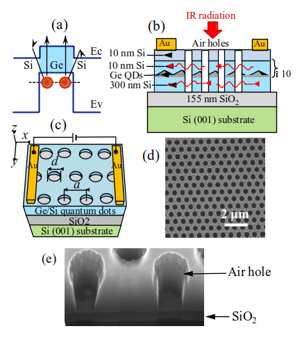 (a) Image of a fragment of the profile of the band diagram of the Ge/Si heterostructure with Ge quantum dots and possible interband electronic transitions leading to the exitation of a photocurrent in the near infrared range. (b) Schematic section of a planar photodetector with Ge quantum dots in a Si matrix on a silicon-on-insulator substrate embedded in a photonic crystal. (c) - Schematic image of a photodetector representing a two-dimensional photonic crystal in the form of a periodic lattice of subwavelength air holes in Si/Ge/Si layers. (d, e) - Images of a fragment (d) of the surface and (e) of the cross-section of a triangular lattice of circular holes in the Si/Ge /Si heterostructure, obtained in an electron microscope.
A.I. Yakimov et al.
JETP Letters 113, issue 8 (2021)